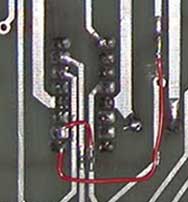
More progress on the SCELBI cassette write board. I have figured out the reason for the rework seen on at least one board.
There are two wires and a cut on this board. In both these cases, the PCB didn’t follow the schematics. Both changes are related to chip Z1 connections.
In case 1, pin Z1-7 should have been connected to Port A, pin T. Port A, pin T is already correctly connected to Z1-13 and Z2-13 and Z2-4. I’m not sure if this omission was on purpose or not. Routing to Z1, pin 7 would require running a trace on the top of board, from Z1-13 out the top of Z1 around the outside of Z1 to Z1-7. This would also require re-routing a couple of other traces on the top side of the board to make room for this new trace. It’s very unlikely, but possible the layout person didn’t want to mess with this and decided to just require the board builder to add a wire.
In the second case, Z1-8 is not connected to Z11-3. Instead Z11-3 is connected to Port A, pin T. The fix requires cutting the trace from Port A, pin T, after it splits and runs through a via to go to Z2. Then a wire can be soldered from the cut trace to Z1-8. This is clearly a layout error.
I still have at least one more mystery to solve on the cassette write board, before I’m done with it, but the layout is shaping up real well.


Pingback: Another SCELBI Cassette Write Board (with logic changes/fixes) « Mike's Hobby Blog