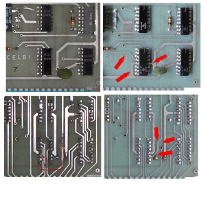
While working on the SCELBI cassette write board, I found some issues which were reported in this blog post. I found that I had detailed images of a second cassette write board, and it looks like the problems on that first board that I looked at, were corrected on the second board.
The first board is the one found at the CHM, and was photographed a while back by Jack Rubin. The serial numbers on the SCELBI associated with that unit are in the single digits, so that unit was apparently a very early unit. The second, corrected board, was part of the collection of Nat Wadsworth. I am only aware of one other cassette interface, but I don’t have images of that unit. I don’t know how many were made before the corrections were made.
Here are partial images of the front and back of relevant sections of both boards. Red arrows on images of the Nat Wadsworth unit show where visible changes were made.
Note that the changes are somewhat different than the what was done in rework on the CHM unit. These changes don’t match the schematics, but I was able to piece together what was done and why.
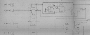
First, let’s talk a bit about what is going on, by reviewing this section of the schematics.
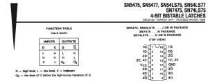
The chip associated with all these changes is a 7475, a part that has 4 bi-stable latches. Here is the key part of the data sheet – the truth table and the pinout.
The function of this chip is pretty simple. Whenever clock input 13 is high, the chip’s output pins, 16 and 15 follow the input on pins 2 and 3, respecitively. Also, output pins 10 and 9 follow inputs 6 and 7, respectively, when clock input 4 is high. When inputs 4 or 13 go low, the associated pair of outputs, are “frozen” or are “latched” into their current state at the time the clocks inputs go low. Note that there are normal and inverted outputs for each latch.
In the schematics, three inputs are connected from a SCELBI output port to this chip. There are two data bits and the port’s output strobe. The output strobe is a high going pulse that occurs when an 8008 OUT instruction addressed to this port. The data bits are connected to the SCELBI write data bus, so will change rapidly, as the 8008 writes to memory or output ports. The strobe is connected to the clock input (pin 13) of the 7475 latches 1 and 2. This circuit allows the 7475 chip to capture 2 bits of the SCELBI output data onto latches 1 and 2 whenever an out instruction is directed to the output port connected to the cassette interface.
What about the two other latches of the 7475? In the schematics, the clock (on pin 4) for outputs 3 and 4 is not connected. What usually happens on unconnected inputs of 74XX series logic is that the input will “float” high. As mentioned before, if the clock inputs are high on the 7475, then the outputs will simply track the state of the inputs. The 3rd latch of this chip is not connected or used. However the 4th latch (pin 7) is connected to the strobe input, so the output will follow the strobe all the time. The inverted output on pin 8 is used as a clock elsewhere on the board. The function is a buffer and inverter of the strobe input to the board. Note that letting an input “float” high is not a good design practice and it’s possible that clock input on pin 4 was directly tied to +5 volts, which is connected to pin 5. It is not connected on the bottom of the board, but could be connected on the top of the board, which is obscured by the chip. The only way to know for sure, would be to use an ohm meter to determine if pin 4 is connected somewhere by a trace that is obscured by the chip. I don’t presently have access to this board, which is in storage at the CHM, so I can’t do this. My best guess, based on the extensive use of pull up’s elsewhere on the SCEBLI boards, and lack of a connection in the schematics, is that it was left to float high and was not connected.
As mentioned in the previous blog post, the first version of the layout has two significant problems.
1) The strobe output wasn’t connected to pin 7 of the 7475. This is rectified with a jumper wire.
2) The output on pin 8 (which is the inverted strobe signal), is not correctly connected to the rest of the circuit. This is rectified by a cut and jumper as can be seen in the image of the back of the board.
So what did the people at SCELBI do, to fix the problems in revised layout.
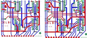
1) Power and ground connections to the chip were rerouted to make room for signal traces that needed to be added.
2) The inverted strobe output which was supposed to be on pin 8 was moved to pin 11, which is the inverted latch 3 output. This was done to make it easier to connect to the rest of the circuit. It was also disconnected from the strobe input connection.
3) The floating clock input on pin 4 was tied to an existing pull up resistor.
4) The latch 3 input was connected to strobe input by running a trace under the chip to pin 13, which was already connected to strobe. I actually can’t verify this change, but I can be fairly certain that it exists, since the circuit would not work without this trace.
Note that this change to use latch 3 instead of latch 4 for buffering and inverting the strobe is not reflected in any schematics that I have seen. The schematics actually don’t match either of the boards described in this description.
If you look at CAD images of this section of the board, you can see how the changes were made. Blue traces are on the bottom layer and red traces are on the top layer of the PCB.
I have repeated this sort of exercise numberous times over the years to solve various inconsistencies in schematics and PCB layouts in a number of vintage computers. Understanding a vintage design frequently requires detailed detective work, but with time and patience, most mysteries can be solved.
One last comment about the nature of the problems with this board. Of the thirteen SCELBI boards that I have investigated in detail, this is the first significant layout problem I have run across. There is an issue on the DBB board with a single missing trace. In this case, the connections to the 7475 were botched and had to be redone. This is a very unusual and unexpected mistake from the engineers at SCELBI.


Pingback: Cassette Write Board Verification in Progress « Mike's Hobby Blog