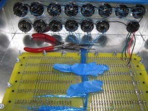
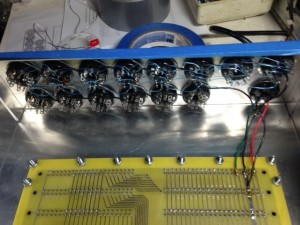
Cassette Read and Write Bringup Status

I’ve spent the last couple of days trying to get SCELBI cassette interface working. Though I have made tapes with the write card, I’m having trouble reading them back with the read card. I’ve also tried some original SCELBI audio files provided by Mark Arnold, but no go on those either.

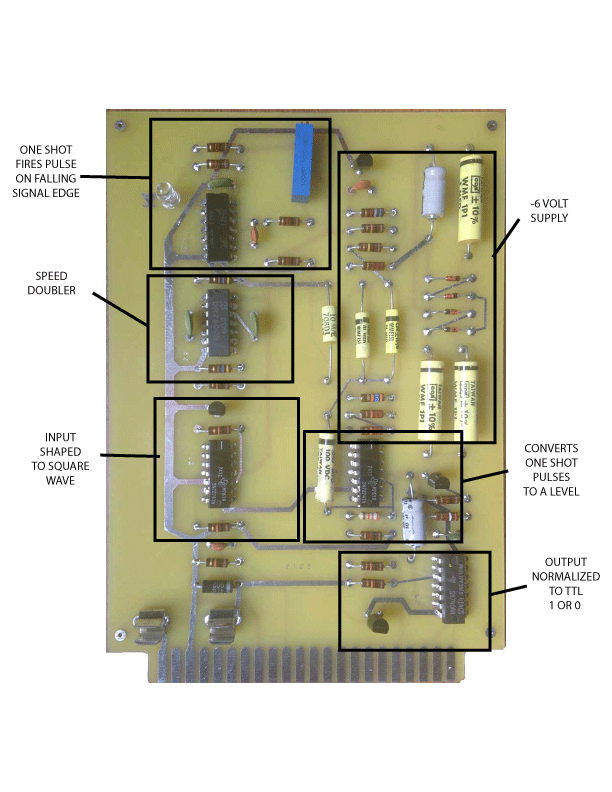
Assuming that my understanding is correct, the read circuit works much differently than what I expected to find. As expected, the first op-amp shapes and filters the signal into a nice normalized square wave. The following gates double the input signal speed and trigger a one shot on each falling edge of this double speed square wave.

Now here is the interesting part. The output of the one shot is filtered and converted into a level by another op-amp. High frequency signals will trigger the one shot more often tending to make the input to this op-amp to average a higher level than with lower frequency input. The output of the op-amp will follow the input. A TTL gate will normalize this output into a TTL one or zero, based on normal TTL level detection on the gate input.

I was expecting this circuit to work like a tone detector, where the circuit only triggers on a narrow range of frequencies. Instead the circuit divides the input frequency range into half and outputs zero on the lower half and a one on the upper half. The demarkation point is pretty much right between the 1350 HZ used for low frequency (zeros) and 2700 HZ used for high frequency (ones). The potentiometer can be used to tweak the center point to some degree. Experiments show that the output appears to be pretty unstable in the middle frequency zone.

There is also a -6 volt power supply built into this card that is used to power the op-amps, so that the card only requires a single +5 volt supply.

SCELBI Read Card Logic Blocks

SCELBI Read Card Logic Blocks

The read program works a bit like a serial interface, by starting sampling on what amounts to be a start bit at the beginning of a burst of four bits. By my calculations, the first bit is sampled after about 2.2 milli-seconds and then a software timing loop samples the incoming signal for the remaining 3 bits at about a 1.5 milli-seconds interval. Each four bit data nibble, is paired with a 4 bit parity and state/status nibble that is encoded the same way. Two such pairs make up a complete byte.

The problem that I’m seeing is that the parity check fails all the time. So far, I can’t find anything obviously wrong, either with read or write, but I have a lot more things to check out before I become “stuck”.

Apple II TTY Emulator Fixed

My previous posts described some barely working attempts at using an Apple IIe as a teletype replacement. When faced with bringing up my SCELBI cassette interface, I decided I needed to improve the Apple II based TTY emulation system.

After spending about a week of my spare time focussed on this effort, I think I succeeded pretty well. The hardware interface hasn’t changed from that previous post, but the TTY emulator now supports the standard SCELBI TTY software and hardware really nicely with full 72 columns and 24 lines. Most of that time was spent trying to overcome what appears to be a glitch in the hardware serial start bit detection.

Except for the initialization routine, I bypassed the Apple monitor character out functions and ended up writing my own output functions. Control characters behave like the SCELBI MEA application package expects them to behave. With the full screen now available, the new TTY emulation software is much more pleasant to use than the previous version.

I didn’t implement a cursor. Some people may feel this is a shortcoming. While a cursor would be pretty easy to implement, I decided that a real TTY didn’t have a cursor, so my emulator shouldn’t need one, either.

If you are interested, the source code can be found at this link:http://www.willegal.net/appleii/ttyemul-fs.asm

While working on this, I found one little issue with the MEA memory dump command. When dumping a full line of memory contents, it attempts to print a space character in column 73 of the TTY. I’d guess that a real TTY would just refuse to advance the carriage in this event. If you know how they really work, let me know.

I’ll need to port these changes over to my RTTY application, so it can also use a full screen. It’s not directly usable, because the RTTY runs at 45 baud and uses Baudot, instead of 110 baud ASCII. In any case, the RTTY port will have to wait, as next up on the to do list, is to check out the SCELBI cassette interface cards, which are built and waiting.

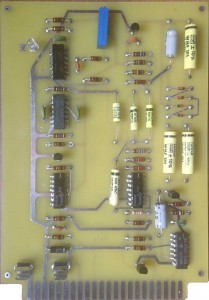
SCELBI Cassette Read Card Built

SCELBI Cassette Read Card

SCELBI Cassette Read Card

Since I didn’t have information on the transistors used, I choose vanilla 2N3904 (NPN) and 2N3906 (PNP) transistors for this build. The 72741 OP-AMPs are vanilla 741 OP-AMPs in a 14 pin package. They are pretty hard to find in that package, but I did manage to snag a few off of eBay. I described where I found the yellow capacitors in a previous post. You will notice one carbon film resistor in the mix. That is because I forgot to order a 2700 ohm composition resistor, and I happened to have the right value carbon film resistor in my stash.

This card is essentially just a tone detector. I should be able to test functionality and performance and adjust it without hooking it up to my SCELBI by using a computer based tone generator application that I bought a while back. This is what I did when resurrecting the HAL ST-6 TTY terminal unit. Except for frequencies used, it basically does the same thing, though at a much less sophisticated level.

One unique thing about this board is that there isn’t a single VIA present.

SCELBI Tape Recording

I made this with a tape recorder this morning.

I will not be able to verify that it’s working 100% until I get the cassette read card built, but it sounds a lot like the sound of an original SCELBI tape that Mark Arnold sent me a little while back.

The format is substantially different than the format WOZ used later on for his Apple computers. The SCELBI actually uses the ones and zeros to switch output between two frequencies, instead of directly generating the waveform in software. This is very similar to how RTTY AFSK (audio frequency shift keying) is done. Though I don’t have the audio format entirely figured out, it appears substantially more complex than the Apple format, with each nibble being sent as a sort of independant packet.

First Reproduction SCELBI Write Card Built

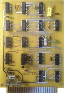
Reproduction SCELBI Cassette Write Card

Reproduction SCELBI Cassette Write Card

Here’s a link to an original write card for comparisions sake.

Except for the relay, I soldered chips directly on the board. Departing from what I did with my SCELBI RAM boards, where I used NOS solder tail sockets, I used a machine pin socket for the relay. No serious issues were found during the build. I powered up and found it draws about .25 AMPs, so I put in a .5 amp fuse. The BOM I published in a previous blog entry was missing a 74121, but I had one of those on hand. I used a 2n3904 transistor to drive the relay and the schematic is missing the value for a 1K resistor. There is a place for a capacitor on the output, but none exists in the images of actual boards that I have seen, so I left it out.

I just noticed I forgot to put in the jumper next to chip Z6.

Outside of some articles in Micro-8 newsletter and some mention in other documents, we don’t have any original documentation for SCELBI peripherals. Once I get everything working, I’m going to have to create some docs for these cards.

After adding the jumper, I’ll build a cable between an edge connector and an 86CP11 connector, so I can plug it in to my 8B and see what happens. I will eventually put it and the read card in an a small aluminum enclosure like the originals had.

SCELBI 8B Working in New Chassis

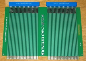
I had a couple of issues. A poorly seated DBB card. This was followed by trouble using the extender card that Cameron Cooper and I had made a while back.

SCELBI card extender

SCELBI card extender

When the extender was added to troubleshoot the DBB card, it introduced noise on the strobe lines, which resulted in issues with my TTY interface. Removing the extender card, and properly seating the DBB card resolved all issues.

Next up: another attempt at printing the front panels and construction can start on the cassette interface cards.

SCELBI 8B I/O Port Wiring Completed

SCELBI 8B Wiring Complete

SCELBI 8B Wiring Complete

I decided to wire the data output bus to the end connector rather than split between the middle two connectors as specified in the SCELBI build manual. I choose to do this primarily because of the cleaner wiring that is possible. The way the data bus is connected to all the memory cards, all the I/O ports and then to connected peripherals through long cables, leaves lots of room for transmission line issues. This concern, is probably why SCELBI recommended connecting four bits to each of the two center connectors. I’m no expert on transmission line theory, so I’m not sure whether the end connection will cause any issues that will require redoing this particular wiring. My guess is that given all the other wiring and relatively low data rate, is that it will have no measurable affect, which is why I’m trying it. The other thing about it, is the idea that I picked up somewhere along the way that branching transmission lines is generally a bad idea. I suppose I’ll have to compare my 8H which was done the SCELBI way with the 8B and see which looks cleaner, electrically.

The other thing I’ve done, is to connect the CPU SYNC clock to pin 10 of input port 3 and pin 10 of output port 3. These are the two red wires, one down the middle of the backplane, and the other from input port 3 to output port 3. Based on my examination of the SCELBI cassette schematics and drivers, it looks like this will be needed to provide timing for the cassette interface.

The last two items before moving onto the cassette interface is checking out the system, now that the I/O is wired and then, finally, screen printing the front panel. I did try screen printing a panel a week or so ago, but had issues with my screen not being stretched tight enough and I’ll have to make another one.

SCELBI Wiring Tips

I’ve had a couple more wiring sessions and only have something like 32 wires to go. I’m doing things a little differently than on the 8H and figured I’d share a few tips.

SCELBI Wiring in Progress

SCELBI Wiring in Progress

First of all, I’m not following the order listed in the SCELBI hardware manual. Here is the progression I’m going through, and why it helps.

  • First, I put in the ground wires. I’m using a little heavier gauge wire on that, and it’s a little less flexible. It’s easier to put in first, because I don’t have to work around all the data and strobe lines.
  • Next I put in the data output bus, wiring pins 1 through 8 from output socket to output socket. These wires are all the same length, so I cut and stripped these wires in batches. Then I did a batch of soldering. I’m not connecting this bus to the backplane, right now. I’ll do that near the end of this process.
  • Next step is the data input lines. Here I have almost completely reversed order from what is listed in the manual. Start with wiring the data bus to port 6. Then work down the line towards port 1. This way, the longer wires go in last, and you will not have to work over and around them, when you solder the shorter wires. The other important change is to wire bit 8 first, working around the connector to bit 1. If you wire from bit 1 to bit 8, as listed in the manual, the higher numbered bits will be harder to wire, because the wires to the lower bits will tend to be in the way of higher numbered bits. This time, I’m paying attention to the manual and using some painters tape to hold the wires down as I work. This keeps things much neater as you proceed. You’ll notice that I also have a needle nose pliers holding down the wires near the sockets.
  • The easiest way to connect the wires to the backplane, is to strip about 1/8″ from the end of wire and use a needle nose pliers to make a small loop, just larger than the size of the pin. Hook the loop around the backplane pin and hold the wire down with a weight of some sort. At that point, you can solder it using two hands and make sure there is no short and adjust it pretty easily. Lead the wire away from the post, and bend it with a needle nose pliers as it works its way to the I/O connecters. Use a piece of painters tape to hold it in place. Cut it to length. Then strip the end and use a needle nose pliers to curve it into a hook shape. Use the hook to connect it to the correct connector pin. This will help hold the wire place, which makes soldering easier.
  • The last wires I’ll do are the data output bus wires and the output strobes. I’ll do these last, so that those wires will not get in the way of the input wiring process which happens on the lower tier of connectors. I haven’t decided how I’ll route the output data lines, but I may route them directly to the output port on the end closest to the data buses location on the backplane.
  • SCELBI 8B I/O Port Wiring Progress

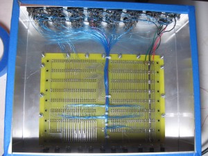
    There are 80 wires to the eight output ports on a SCELBI, and 54 wires to the six input ports. All wires must be cut to length, stripped and soldered by hand. This wiring is, by far, the most tedious and time consuming single task involved in building a reproduction SCELBI. When I wired the I/O ports on my SCELBI 8H, I did it in one marathon session that took almost an entire day. For my 8B, I’m not in so much of a hurry and so far, have had 3 shorter sessions and have 56 of the 134 wires connected. The connected wires are all the ground wires for both input and output. I also have 6 bits out of the 8 bits of the output port bussed together, but not connected to the backplane. For connecting the output data bus, I found I could cut and strip a batch of equal length wires, then solder them between connectors.

    SCELBI 8B I/O Port Wiring in Progress

    SCELBI 8B I/O Port Wiring in Progress

    The blue painters tape is there to protect the edges of the enclosure while the system is being constructed. I think another three or four sessions and I’ll finally have the wiring task done.

    SCELBI Over Current/Over Voltage Protection

    Each SCELBI board is protected from over voltage and over current with a fuse in series with a zener diode. For 5 volt supplies I use 1N5341 6.2 volt zener connected between the 5 volt supply and ground. For -9 volt supplies I use a 1N5349 12 volt zener connected between the -9 volt rail and ground. When the voltages are at normal values, the zeners do not conduct and remain inactive, not affecting the circuit. If the voltage exceeds 6.2 volts (on the 5 volt supply) or -12 volts (on the -9 volt supply), the zeners will start conducting, acting something like a short. This should prevent the voltage from rising any further above the switch on value of the zener, preventing damage to the circuitry. Also, if there is enough current, the fuse in series with the zener should blow, removing power altogether and saving the circuitry.

    The main concern with this sort of circuit is that the zener cannot conduct infinite current for an infinite amount of time, before the zener itself acts like a fuse and blows. Once the zener blows, there is nothing to prevent the voltage from rising and destroying other components on the card. This is one reason that the SCELBI has different fuse ratings on different cards. The sooner that the fuse blows, the less likely that the zener will fail, first.

    The 1N53XX diodes that I use on my reproduction SCELBI are not the same devices that were originally used. Though the 1N53XX devices have pretty good current handling capabilities, I was never quite positive that they would outlast the fuse in the case of an overvoltage event.

    Last week, I decided to do a simple test in order to convince myself that these zener diodes would do the job in the case of a problem. The test I put together was quite simple. Simply connect a lab power supply to a fuse and a 1N5341 zener in series. Then crank up the voltage and amperage on the power supply and see if the fuse or the zener failed first. If the fuse went first, I knew the solution would be fine.

    I started with a 1 AMP fuse. Adjusting the voltage to something greater than 6.2 volts and turning the amperage up to 1.5 AMPs resulted in a fuse that blew right away. Then I connected a 3 AMP fuse to see how the zener would fare under extended load. I didn`t leave the power supply on for too long, but the zener seemed to survive short tests without a problem. Finally, I turned the power up to 5 AMPs to see what would happen. After a few 10 second tests neither the zener nor the 3 AMP fuse blew. Since I didn`t really want to destroy the zener, I called the test a success.

    The 1 AMP or smaller fuses used in the SCELBI would certainly blow before the zeners that I am using. As long as you use the correct fast blow fuses, I am quite comfortable recommending the 1N53XX series zener diodes for over voltage protection on the SCELBI cards.