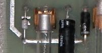
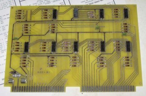
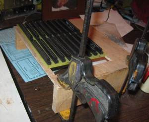
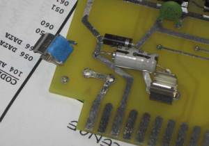
Last Friday, I thought I froze the layout for the final time. I took a few looks at it, checking for correctness over the last week, finding nothing to fix or improve upon. Today, I planned on kicking off the build, after doing a final check. However, during this “last” check, I noticed that the diode symbols were missing on the front copper layer. The are not obvious, as they are obscured by the actual diodes. I’ll have to add them in, recheck the layout, regenerate the Gerbers and do some final checking (yet again). Hopefully the PCB will be ready to order by Monday. After that, it will take about four weeks, plus or minus, to be manufactured, shipped, built and tested.
Category Archives: 8008
Memory Test for the 8008 Posted on my 8008 Software Page
This was ported to the 8008 from my 6502 memory test program by Mark Arnold. I have made some modifications to his port, so any problems are solely my fault.
It contains a couple of enhancements over the 6502 version.
http://www.willegal.net/scelbi/apps8008.html
By the way it’s been running for the last hour, checking out the 12K of memory installed on my reproduction 8B, without reporting any errors.
I suppose someone who needed a good 8080 memory test could port it to the 8008 or Z80 without too much trouble.
What is SCELBI’s MEA
Like so many other things in the SCELBI world, it’s best to let the creators describe it for you.
THE SCELBI MONITOR/EDITOR/ASSEMBLER PROGRAM, ABBREVIATED IN THIS MANUAL AS “MEA” IS A POWERFUL SOFTWARE PACKAGE THAT COMBINES THE FUNCTIONS OF A MONITOR, EDITOR, AND ASSEMBLER IN A RESIDENT, CONVERSATIONAL TYPE ARRANGEMENT. THE PACKAGE IS STANDARDLY SUPPLIED ON A PROGRAMMABLE READ ONLY MEMORY ELEMENTS THAT RESIDE ON PAGES 60 THROUGH 77 (OCATL) FOR USE IN A SELBI-8B MINICOMPUTER. I/O ROUTINES FOR THE PACKAGE ARE SUPPLIED ON TWO SEPARATE “PROMS.” THE STANDARD SCELBI AUDIO TAPE DRIVING PROGRAM RESIDES ON PAGE 77. I/O ROUTINES FOR THE SPECIFIC I/O HARDWARE TO BE USED WITH THE SYSTEM IS PROVIDED ON A PROM ON PAGE 76. TWO STANDARD I/O VERSIONS ARE AVAILABLE. ONE FOR SYSTEMS EQUIPPED WITH THE SCELBI OSCILLOSCOPE ALPHANUMERIC DISPLAY INTERFACE AND SCELBI ASCII KEYBOARD INTERFACE, THE OTHER FOR SYSTEMS USING A MODEL 33 TELETYPE INTERFACED WITH THE SCELBI BIT-SERIAL TTY INTERFACE. OTHER TYPES OF I/O DEVICES CAN BE ACCOMMODATED BY SPECIAL ARRANGEMENT AND SUBSTITUTION OF APPROPRIATE I/O ROUTINES PROGRAMMED ONTO A PROM ON PAGE 76.
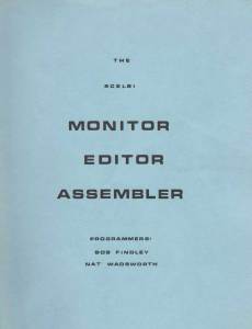
Here is the cover of the manual, which can be found at scelbi.com.
This development environment, which was available in 1975, was quite an achievement for the time. The environment was “robust” enough that Mark Arnold used it to develop SCELBAL. Few other “personal” computer systems available in 1975 had such capabilities built in. For instance, Microsoft BASIC for the 8080/Altair was developed in emulation on a PDP-10.
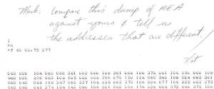
Also at scelbi.com is a intel hex file of the contents of the PROM card. This version of the contents was painstakingly reconstructed by Mark Arnold from an object listing that was sent from Nat Wadsworth to Mark when Mark started experiencing problems with the EPROMs on his system back in the old days. It’s very fortunate that Mark saved this listing.
The listing was just a raw dump and where it was folded the data was illegible. Mark and Cameron Cooper managed to get MEA up and running in emulation and used the emulator to help reconstruct the missing data, so they believe the hex file at scelbi.com is correct.
The version they have, is set up for the TTY interface. So far, we haven’t been able to find a surviving version of the oscilloscope drivers that would replace the TTY drivers on page 76. I think it’s rather unlikely at this point that we will be able to find the oscilloscope version, so that version will most likely have to be rewritten from scratch.
We have the TTY version of the MEA program and I have already done the TTY interface card, so we are getting close to having reconstructed a complete SCELBI 8B running MEA. After completing the PROM card, my next efforts will be to do the cassette interface, which will allow running the MEA system as it was intended on real hardware.
In order to get MEA working in my OS/X emulator, I’ll need to enhance the terminal support to act more like a real TTY as CR and LF are separate functions and I’ll also need to figure out how to support backspace. I also intend to add cassette interface emulation support to my emulator to allow complete support of MEA in emulation.
Reproduction SCELBI 8B now running SCELBAL
This has been a very long time coming and I’m super excited to see it finally running.
Here is a very poor quality video of it in action.
Note that the versions of SCELBAL found on the net require 12K because they include all the available features and options. In order to run in a 8K system, the array feature is going to have to stripped out.
A SCELBI 8H-B
I’m calling a SCELBI 8H that includes a 4K memory card from a SCELBI 8B a SCELBI 8H-B. See the original 8H-B here.
Attaching a single 4K memory card to an 8H is easily done because of the way that SCELBI memory cards are addressed. While reading the following description, keep in mind that on a SCELBI, a bank of memory is considered 256 bytes.
On a SCELBI 8h, there are 4 bank select lines connected to each slot for a total of 16 bank select lines. This provides addressing for 4 banks or 1K per slot and 16 banks or 4K for the entire system. The are 4 bank select lines connected to each of the 4 slots at different points as can be seen in this image of part of the 8H backplane.
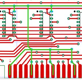
On a SCELBI 8H 1K memory card, each of the four banks available on the 1k card, is connected to the backplane at four different points. In the picture below, the line for the first memory bank on that card is highlighted in green.
Depending upon which slot the card is plugged into, it will pick up the 4 bank selects for that slot, thus automatically providing a different address range for each slot, without requiring extra decoding logic on a memory card.
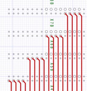
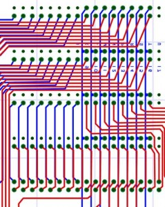
The SCELBI 8B memory design is a little different in that the memory expansion card decodes 16 banks for each slot (4k) and a total of 64 banks (16K) for the entire system. This image shows the 64 bank select lines going to the 4 memory slots on a SCELBI 8B backplane.
The 4K memory card is also different, with the 16 bank lines all feeding into the on board circuitry separately.
This design also requires extra complexity on the memory card. The 16 bank selects on the back plane must be demultiplexed into 4 chips selects, each of which selects one of the four rows of memory chips.
So how do you connect a 4K SCELBI memory card to the 8H? A few of you may have already deduced how to do this. You simply jumper all 16 banks selects available on a 8H backplane to a single slot, making sure you leave the other slots empty. This still leaves you a 4K system memory capacity, but will significantly reduce the cost of creating a 4K SCELBI 8H.
The SCELBI 8B memory addressing architecture is unique in my experience. I think it was deliberately designed to allow use of a single 4K memory modules in a SCELBI-8H. Perhaps Nat and Bob were considering a cost reduced 5 slot SCELBI 8H backplane that would take advantage of this architecture.
SCELBI 8B Early Adopter PCB Sale
I am now offering 8B PCB set to early adopters a special price of $275 plus shipping. Though my prototype system has been brought up and basically checked, it hasn’t been fully checked with a full complement of memory and PROM cards. Also I/O port testing has been minimal. There could be additional issues beyond those already documented in my blog that will require rework. Once checkout is considered fully complete, the price of a board set (minus PROM card) will rise.
The introductory set contains one each of the following PCBs. Extra SRAM cards are available now at $50 each. This set does not include the PROM card, which is still under development. Estimated time before PROM card will be available is 3 months, give or take 2 or 3 months.
1100 CPU
1101 DBB
1102 INPUT
1104 Front panel
1106 memory expansion
1107 4k SRAM (1)
1108 8B Backplane
Send an email with your address and and questions to:mike@willegal.net for a shipping quote and ordering information.
I’m not sure when chassis sheet metal will be available, as I’m looking for bargain on a used Box and Pan Brake, so I can fabricate them at substantial savings over contractors prices. Note that not just any brake will do, it has to handle a minimum of 2′ of 16 gauge stock with at least a 4″ depth. for now, you can fabricate your own temporary chassis or use an off the shelf Bud AC-413. The only problem with the Bud chassis is that the original chassis were 3.5″ high and the AC-413 is only 3″ high.
My Improved Understanding of the SCELBI Data Display
During my debug of the 8B, over the last couple of days, I improved my understanding of the data display on the SCELBI front panel. Though it is clear from the block diagram, some things just don’t sink into my brain without some additional lessons, usually learned the hard way.
The data display simply shows the contents of the memory location that is currently being addressed. I already knew that when you stop or step the SCELBI, it stops after setting up the address bus, but before executing the next cycle. In 8008 terms, this is at CPU state T1. The two status bits on the front panel are simply the two high bits of the high byte of the address byte. These two bits are not actually address bits, but known as the cycle control decodes, which is why the 8008 only has 16K of address space and not 64K. Another fact to consider is that both 1101 and 2102 memory chips have different input and output data lines.
The interesting thing that is a result of these design decisions, is that you can do simple memory tests from the front panel by writing a memory location, without even reading it. The data you write should show up on the front panel, without the need to even execute a read instruction. If you have a write failure, you will immediately see that the data you thought that you wrote is being displayed incorrectly and therefore has been written to memory incorrectly.
One other thing, without memory in the system, the data display will always show up as all ones. You can still jam instructions into the CPU, but you will not be able to use the data display as an aide to troubleshooting.
8B Running Tiny SCELBAL!!
I need to build another memory board before I will be able to run the floating point version of SCELBAL. I think I have most all of the parts on hand for at least 1 more board, so this shouldn’t take too long.
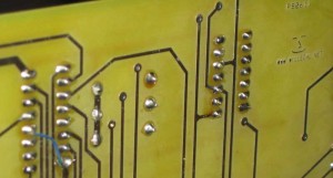
I had to debug two problems. First was a missing trace on the memory expansion board. This ran under the 7442 located at Z9 from pin 12 to ground. During design checks I check every pin on every chip for a connection to the correct net, but I missed the ground connection on this pin. The trace is completely obscured by the IC, so it’s invisible in images. It is documented in schematics and I probably should have caught it during design checking. Anyway, it’s not serious enough to qualify for a respin of the board, since it can be fixed by running a ground wire under the chip from pin 12 to pin 8 before soldering it (or the socket for it if you decide to use sockets) to the board. This fix will be practucally invisible to anyone inspecting the board.
The other issue was a pin bent under a memory chip. This took longer than the missing trace, as I was assuming that something was wrong with the soldering or layout on one of the boards.
I have done some rudimentary checkout of all the memory slots (with my 1 board) and so far they all look functional. The last slot was only half checked out, due to the lack of another 7442, which I haven’t gotten yet. I will not feel like that the system will be fully checked out until I get 3 memory plus prom board all working together. However, I’m confident enough that it will be ok, that for those of you that want to start building a SCELBI 8B, I’ll start a discounted early adopters program in the next couple of days.
Reproduction SCELBI-8B Power On
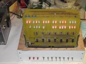
Finally powered on. Still need to add and test memory expansion and memory card, but I can jamb instructions with the front panel. I’ll start checking out the memory as soon as I finish this post.
While wiring the backplane, I found that SCELBI made a change in the RDYN jumpering. Instead of jumping XA02 A-X to A-Y and A-Z, the 8-B instructions connect XA02 A-X to A-Z and connect XA02 A-Y to B-F. I’ll find out as the day goes on, if that makes stepping any more reliable. If so, it would make a good change for the 8-H, also.
The chassis was hacked together out of wood and sheet metal. I’m looking into finding a used Box and Pan brake so I can cut and bend my own chassis. The ten Bud chassis’s Corey had made for the 8H project cost $1000, and that left no room for profit, so he sold them at cost. Also, I want to make chassis for the expansion cards and power supplies. The whole thing just adds up to too much expense. Also if I had them made, when the batch is sold out, then future SCELBI builders are left without options, cause I can’t afford to buy ten and have nine sitting around for months.
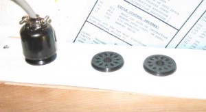
For the prototype, I’m just wiring up 1 input and 1 output bit, so I can download programs and use a terminal. Here is the back panel.
SCELBI 8B Progress
Memory Expansion Board is almost done – I’m short one 7442, which will prevent me from checking out the last slot, but otherwise it’s ready to go. This board went pretty quick, the 67 resistors took as long as anything else on this board.
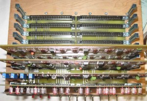
For now, I’m hacking together a wooden chassis with sheet metal front and rear panels. Once I get the aluminum version figured out, It will be easy to move the backplane and front panel switches from this hack job to the final chassis.
As far as the possibility of the short on the 4K SRAM board, though it’s pretty remote, I decided to add some masking tape to the bottom of one end of the fuse holder to eliminate it entirely.
Given where I’m at at this moment, I expect I’ll be able to power up the 8B with 4K of SRAM within a week.

