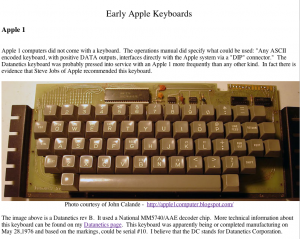
Just added the first version of an early Apple keyboard page. This details some of the changes that went into early Datanetics and Apple keyboards. There are more keyboards to be added, but I figured that I had enough interesting stuff written up to put up this link.
Category Archives: Apple II
Apple II rev 0 closeout results
My ebay A2 rev 0 replica motherboard closeout on ebay is done. I successfully sold 4 kits for an average price of a bit under $300. Subtracting ebay fees, paypal charges, the net take was similar to the cost of putting these kits together.
However since my motivation was to bring in some cash, so I could move some other projects ahead, I consider the sale a success. The money is earmarked to make my Datanetics keyboard replica project a reality.
The ebay sales indicate that the current fair market price of the these kits is just under $300. Given that the cost of putting together kits is nearly as much, it is just not economically feasible to sell these kits. Maybe someday in the future things will change, but that is how it looks to me at the moment.
Here are some facts about the A2 rev 0 project.
Motherboard laid out 1st half of 2007
First board brought up summer, 2007
Last kit shipped fall, 2010
Production run:
2 batches total of 18 boards
1st batch 6 boards (glossy solder mask)
2nd batch 12 boards (matt solder mask)
Kits sold – 14
Bare boards sold -1
Build and tested motherboards sold – 1
Built and kept -2 (one from each batch)
I was hoping that the profit from this effort would be enough to pay for an original rev 0 or perhaps one of Grant’s Altair kits (no longer available). Though, financially, I did just a bit better than break even, the main profit came in other forms. I had a great time with this project. I made some great friends. I learned a ton about PCB layout and working with various suppliers. Also, I don’t think I could have done the more difficult Mimeo PCB as well as I did, without taking on this project, first.
Finally for those of you interested in the Mimeo kits, don’t worry, I will continue to produce and sell these kits as long as there is continuing interest and components available.
What O’scope Should You Buy?
I recently received this question from a fellow retro-computer hobbyist. Since it was such a good question, I figured I’d post my reply here on this blog. Though I can’t make a specific recommendation that is right for everyone, here is how I responded to this inquiry.
I use an old 100MHZ Tek 465 that I picked up off of ebay for about $80 (shipped). I was lucky, and it was almost completely functional, when it arrived. I spent another 50 bucks on probes and some minor repairs (replacing broken knobs). Total cost was less than $130.
Prior to landing this unit, I would occasionally borrow a more modern HP 20MHZ 4 channel digital storage scope from work. The user interface was nice and storage was great to have, but the bandwidth was a bit limited, considering early Apple computers have a base 14MHZ clock.
At times, it wouldn’t hurt to have more than 2 channels and occasionally a little more bandwidth would help. So I guess I think that 100 MHZ, 2 channels is minimum for my purposes. 100MHZ sounds fast, but remember that you want to see glitches and signal slope, not just digital highs and lows. The real neat thing about using this old scope is that this same tool was in use in the 70’s and 80’s by developers of the first personal computers. The price was right, too. At the time I bought it, I don’t think that you could touch the bandwidth at that price any other way.
A modern digital storage scope would be easier to use, especially on transient signals, as the scope stores the capture and you can view it at your leisure. On a traditional analog scope, a transient just flashes on the screen and is only present as long as the screen phosphor glows (one shot).
There are also digital storage scopes that plug into PC’s USB port and use the PC as the brains and display. Some of them have logic analyzer functions, which would be nice to have. Many of these units have limited bandwidth, compared to my old 100MHZ Tek.
I guess the bottom line is you need to decide much you want to spend and what kind of features are important to you.
Apple II rev 0 inventory cleanout
Apple II rev 0 kits sales have been extremely slow. I have quite a bit of money tied up in parts and boards for the rev 0 and I have some other projects in the pipe that I would like to spend some of that money on. In order to facilitate this, I’ll be liquidating my rev 0 stock of kits on ebay. I have 5 kits on hand and will be posting them for auction one at a time.
After this liquidation, I don’t expect that I will be offering A2 rev 0 kits for the foreseeable future. There is some possibility that I might get a batch of motherboard PCBs made at some point down the road, but only if I notice some demand building up. Unless something significant changes in terms of this market, I don’t think that I will offer kits, again – only bare motherboards and possibly built up computers.
I really wanted to keep this product alive and available for as long as I could find parts. However the demand just isn’t there and I’ve have some ideas for some other projects that could use the money that I have tied up in these kits.
New Apple 2 Rev 0 Revelations
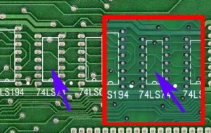
I did a comparison of the hidden traces on my rev 0 replica with the fantastic image of the front bare Apple II rev 0 PCB, that I just received from Stanford University. I found that all of these “hidden” routes were precisely the same as the actual rev 0, except for two.
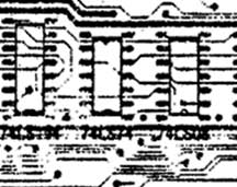
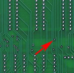
The image on the left, is the original. Note that this missing trace is actually an undocumented bug in the rev 0. The trace connects the D input of a flip flop with a pull up. Without the D input to the flip flop being pulled up, it is left in a “floating state”, That means that when a clock edge is seen on the flip flop, that either a positive or negative level will be clocked in, depending on exactly where the input is floating at. Usually this will be a positive level, since 74LS input logic tends to float high, but it’s far from guaranteed. This flip-flop is used to indicate to the computer when a character is pressed on the keyboard. This floating input could cause the computer to miss keystrokes. I don’t remember this being a problem on my original rev 0, but the possibility is there.
When laying out the replica PCB, I ended up cutting up a socket on a later rev board in order to determine the route of this trace, not realizing that it wasn’t even present on the rev 0. The poor photocopy in the “RED BOOK” occasionally wasn’t good enough for me to solve a puzzle, and I had to resort to this sort of tactic, from time to time. In this case it failed me. Looking at the image now clearly shows that the trace wasn’t present, but there are other places on the photocopy where present traces are barely visible. For some reason traces that ran vertically often show up poorly in this photocopy.
It you have one of my replica’s and want to experience authentic behavior, lift pin 12 of the flip-flop out of the socket (or you can bend it under so the change doesn’t look obvious). You probably will not notice any difference in behavior. You could also cut the trace, but I would recommend that you leave well enough alone and run it as is, with the input properly pulled up.
The routing of trace in question is partly hidden by the ear of the slot 7 connector. I connected pin 39 of the peripheral bus, USER1, from the peripheral bus to the wrong via. This via directly connects to the enable on H12. USER1 should have connected to another via, that is not connected to anything else. The user was supposed to add a jumper between two vias to make this connection.
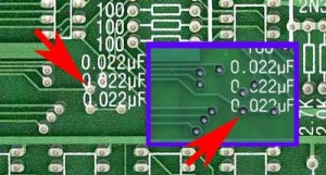
If you have one of my rev 0 replica’s I would do nothing. I have heard of no issues of peripheral card compatibility from replica builders over the years. You are more likely to have peripheral card problems because of the other changes that were introduced to the bus than with USER1 being connected to the enable of the decoder at H12.
There is a very minute possibility that you may have an issue with an unusual peripheral card that uses USER1 in an unexpected fashion. In this case, you can disconnect USER1 by carefully cutting the trace on the back of the PCB that leads from pin 39 (USER1) of the peripheral bus to the via that takes to the trace to the front of the board. Instead you could try cutting the trace where it connects to the via near the edge of the slot 7 connector. This will be more difficult because the ear of the connector partly obscures the via.
Stanford University’s “Apple 1”
Turns out that the Stanford “Apple 1” is an unpopulated Apple II, rev 0 PCB. The only other unpopulated A2 rev 0 I know of, is the one that the Hudson Brothers just sold. As rare as this is, it would have been nice to find a bare board Apple 1. By the way, during this investigation, an archivist at Stanford Library sent me the best image I’ve ever seen of the front of a bare original Apple II rev 0 PCB. More on that in the next post.
PS/2 Keyboard Interface Design Decisions
Someone sent me an email asking if I could have created a PS/2 adapter that was reconfigurable in software to work with either an Apple 1 or Apple II with no hardware jumpering. I started to compose a long answer and before sending it, realized that this would be a good blog entry. So here it is.
The AVR to DIP wiring mechanism was the most difficult part of the design process, for the PS/2 keyboard adapter.
First of all I couldn’t do a software switch between the A1 and A2 pin outs without some external power switching circuitry, as the power and ground connections are different. For example, minus 12V on the Apple 1 is connected to the same pin as a data bit on an A2 keyboard.
I wanted to support S-100 and other systems with possibly different pin outs, with a standard ribbon cable. I thought about creating a user interface with the serial port to allow tweaking configuration, but decided it was too much work and could cause too much confusion, if configured wrong.
I was also concerned about increasing potential for bugs. The code for the PS/2 keyboard is pretty complex, as it is. Besides doing the bit banging to move stuff over the wire, you have to keep track of key states. Some single key state changes result in 3 bytes being transferred to the adapter. You don’t really know what is going on with the keyboard until all three bytes are recieved. When you finally decide that you have a character for the host, you then have to map a generic key code into an ASCII equivalent. A depressed shift, control or other key affects the translation.
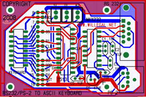
I actually laid out at least 3 variations of this board over the past couple of years. First version was a single sided PCB and A2 specific. This one can be seen at the bottom of my keyboard adapter web page. The next version was A2 specific, but you could cut existing traces and add jumper wires for other systems. Here is a CAD image of this version.
The Data bits are optimized for the A2 connection, not ease of wiring. Notice that I also reversed connector ends between this version and the final version. This was to make the ribbon cable connection between an A1 and this adapter more straight forward. I think that in most cases with an A1, the adapter will be to the left of the motherboard. With the original configuration this would require twisting the ribbon cable to connect correctly.
Finally, I decided I needed to create the most generic version possible, because of the desire to support systems which could have any sort of pin out. I considered making it default to A1, and then allow cutting traces and adding wires to adapt to other systems, but decided that cutting traces was destructive and not very elegant for non-A1 applications.
Once I decided that I didn’t want to force non-A1 folks to cut traces, I rearranged the pads and pin out to make hookup as straight forward as possible. I think in this regard, I succeeded. When I wired my first boards, I found it much easier to do, than when I built a wire wrap A2 keyboard to A1 converter using two wire wrap sockets. I also figured that it was going to be sold as a kit. A little extra work on the kit builder’s part, really wasn’t necessarily a bad thing. 🙂
I guess this long winded blog indicates how much I thought about the problem. The optimum design would to make a different board for each application, but it would not have been economically feasible.
I’m very happy with the result and have been exclusively using a PS/2 keyboard with my A1. The long cord and keyboard layout is much more user friendly than using an A2 plus keyboard with ribbon cable connection.
Get your Mimeo 1 or A2 rev 0 replica, signed by WOZ
Cameron Cooper had his Mimeo 1 signed by WOZ. I had another Mimeo 1 builder mention that he was going to have it done, as well. This second builder pointed out the web site that offers the mail in service.
On the site, there happens to be a picture of WOZ signing Cameron’s Mimeo 1!
http://www.signedbywoz.com/shop-mail-in.php
Note that Cameron was told that this was the first replica Apple 1 that WOZ has seen. It seems that it will not be the last.
I’m tempted to send in a batch of bare boards, but I’ll leave it up to the replica builder to decide whether it is worth the trouble or not. I’ve already spent enough money on this project.
Apple Cassette Interface Revisited
Yesterday, I spent the good part of the day with the ACI and finally have a good fix that makes it far more robust without changing the board layout. In the past I had discovered that the Apple II cassette interface is far more reliable than the Apple 1 was. I did spice simulations of both and quite a bit of fooling around with the actual ACI in order to see if I could figure out the problem. The best improvement I could come up with, was to add a low pass filter on the input. This was done by adding a .01uF cap between the input side of the comparator and ground.
In revisiting the ACI yesterday, I finally discovered the real difference in the design that makes the Apple II so much more reliable. The Apple II uses a .1uF capacitor for input coupling versus a .01uF on the ACI. When I looked at this in the past, I must have forgotten to make this change when evaluating the designs with spice. This change provides a lot more noise immunity in the comparator inputs.
Here is the ACI input signal with the stock .01uF input coupling capacitor. The source of the signal is the 1HZ tone (all ones) at the front of Wendell Sanders Hammerabi clip being played from an iPod with the equalizer set to “treble reducer”. All signals are displayed at .5 volts/division on this page.
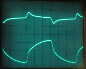
In the image, above, the input is the bottom signal and top signal is how it is presented to the comparator input after passing through the capacitor. Note how the signal spikes and then returns to the value set by the 10K resistors.
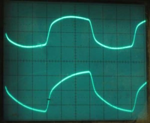
Above is the same input and output signals with a .1uF capacitor. The signal follows the shape of the input waveform much more closely. The bottom trace is input signal and is the same as in the first image. The top trace is input to comparator after passing through cap. Note how the extra capacitance prevents the resistors from quickly returning to the base value set by the resistors.
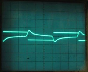
This image shows both inputs to the comparator with the stock .01uF capacitor. Spiky looking trace is input signal to comparator (same signal as seen in first image). Other trace is reference signal with hysterisis. The reference signal is pulled up and down slightly as the comparator switches state to prevent instability. This results in the square wave.
In the picture above, the output switches state when input signal (more spiky looking signal) passes the level of the reference signal as can be plainly seen in this image. The problem with this design is the limited amount of room between the input and the reference, any input noise with an amplitude of around .2 volts or more may be enough to trigger a switch in output levels.
Below are the same two inputs to the comparator with the .1uF cap. This wave form increases noise immunity to almost a volt, about 5 times improvement over the apple 1 stock implementation.
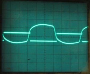
Unless you are interested in maintaining complete commonality with the original Apple 1, I highly recommend using a .1uF capacitor in your replica cassette interface instead of the .01uF used in the original design. Keep in mind that the folks at Apple recognized this improvement before coming out with the Apple II, as that design includes .1uF cap for this application.
Since I was using a clone ACI, built with components based on the schematics, I wondered if Apple actually shipped with .1uF caps on the ACI. I exchanged a couple of emails with Wendell Sander. He confirmed that the schematics are correct and the Apple ACI did indeed ship with a .01uF caps. He also confirmed that he had independently come to the same conclusion regarding the reliability improvement that could be attained with a .1uF cap.
PS/2 RS232 to ASCII Keyboard Adapters Now Available
Go to this web page for details:
http://www.willegal.net/appleii/appleii-kb-int.htm
In my opinion, building one of these adapters is not very difficult. I have been able build and test one of these adapters in about an hour.
If you can get a piece of Apple 1 software into Apple Monitor Command format, I believe that this RS232 interface is one of the most straight-forward ways to download software from a PC to your Apple 1.

