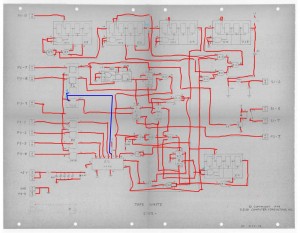
Verifing the layout against schematics, is an important step in my reproduction process. My usual method of schematic/layout verification is to print a copy of the schematics then mark each trace as I verify the connection with a marker. This time I did it all digitally using photoshop as a replacement for the paper.
The blue layer notes omissions, corrections or clarifications to the schematics. Most of these are due to the mistakes made in the initial rev of the board, which were later corrected. The version of the schematics I have access to, does not have those changes incorporated into them.
During this process, I did find a number of traces that were hidden under chips. Omitting these traces is an easy mistake to make. I missed one of these on the memory expansion board. This time, I am reasonably sure that I found them all.

