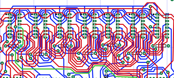
I’ve been working on reproducing the a copy of the Digital Group video card. In the process, I have found that the layout of the board is pretty convoluted in some places. In particular, the layout for the seven 1101 memory chips is pretty messy. Though, it is far from complete, the traces are all in place and you can see approximately what this part of the completed design will look like by viewing the following image.

Take a look at how the traces wind around the outside of the chips. Circuit board design was done by hand back in those days. The layout is made by making an image of the PCB on a piece of film that will be reproduced by photographic imaging. Each small section of straight trace is laid onto a piece of film by cutting an appropriate length of tape and laying it down on the film. Though the size is typically 2X the final size of the PCB, which makes things a little easier, it is still a time consuming process. With this many changes in direction for each trace, I can’t imagine how long it took the layout artist to produce the original artwork. Even digitally, it is taking quite a while for me to reproduce.
For quite a different approach to the same problem, take a look at the layout of 1 bank of the SCELBI 1K SRAM card, which uses the same 1101 memory chips. In this case almost all traces run in straight lines, making for a much easier layout process.

So why is there so much a difference? The Digital Group card has absolutely no traces running between the pads of a chip. I presume they did this in order to make the design a little more robust as tolerances can be a bit tight when you run traces between the small gaps between the legs of a chip. Tight tolerances can result in higher likelihood of PCB manufacturing defects or solder shorts during the assembly process. However, by making the small sacrifice of tighter tolerances, you can see that there is great improvement in the resulting design.
